
The Project: Motivations Specifications Current Focus Front Panel Logic Events: VCF East XIII VCF West XIII DEFCON 26 VCF Midwest 13 VCF East XIV VCF West XIV VCF Midwest 14 The Future: Want a Cactus? |
|
It started out as an idea.
It's taken a pile of paper and lots of research to get this far. I've spent months of time working on it. I've run digital logic simulations, and revised my designs time and again. I've had help from a handful of friends, plenty of acquaintances, and a smattering of strangers. I've experienced countless failures and setbacks, and sacrificed more sleep than on any previous project I've embarked on. But it's all been worth it.
|
What's the point of all this?
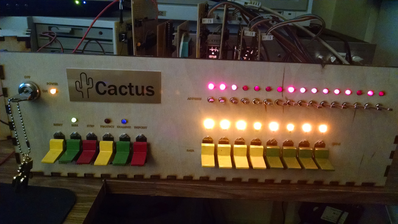
The Cactus is a computer, built with the goal of recreating the homebrew computer experience of the 1970s. This includes hand-wired circuit boards, 7400-series logic chips, and only a few post-1980 concessions where appropriate. While many machines of that era were commonly found with a front panel interface, only a few obscure examples use a 6502 microprocessor. Initially, the Ohio Scientific OSI-300 was the only exception that I was aware of. I first saw one at Vintage Computer Festival East X in 2015, at Bill Dromgoole's exhibit table, and it sparked a wave of curiosity and possibility -- but back to reality. The OSI-300 was never intended to perform any sort of practical computing. Rather, it was a bare-bones trainer to introduce the user to the 6502 opcodes.
This is certainly not the only 6502 front panel computer in existence. There is a variant of the CGRS Microtech System 6000 which is an S-100-compatible system that had an optional front panel DMA board. I previously thought this was intended for a SYM-1, or another CGRS Microtech S-100 option, but it's more like a stand-alone system. I've also learned about a 6502 homebrew design found in Byte Magazine known as the the Kompuutar. I would be surprised if any surviving examples of this machine exist, since they would have all been hobbyist made. All three of these examples are obscure, and didn't achieve much commercial success. Not to mention, they're all bundled with heavy limitations.
It was far more common to find 6502 processors with ROM monitors, hexadecimal keypads, and 7-segment displays, exemplified by the MOS Technology KIM-1, Synertek SYM-1, and Rockwell AIM-65. Then the microcomputer boom of 1977 changed the game entirely, and the front panel's time had come to an end. Graphical interfaces with keyboards became the norm, but I digress. I've used the modern Mini OSI-300 replica in lieu of a real one. The Mini OSI-300 recreates the experience while upgrading the SRAM from 128 bytes to 4K, all while having a smaller device footprint. The hard part is using such tightly packed switches, and my fingers get tired of it really fast.
Time to build a computer:
The primary CPU/RAM/ROM/UART interactions are based on Grant Searle's Mininal 6502 design, modified for use with a bus structure. Quinn Dunki's Veronica has served as major inspiration, particularly in her approach to construction and single step operation experiments . I took inspiration on front panel operation and interface design from slews of 1970s minis and micros. The front panel logic is very much my own original work. It takes about two dozen 74HCT series logic chips to make up the front panel control logic. Previously, I was using a variety of other 7400 series logic families, but switched to HCT at the suggestion of the good folks at 6502.org. The result is a colossal pile of wires that actually runs.
Other modernization choices made include the use of a single SRAM chip containing 32K. The historically accurate solution would have been to use boards and boards of DRAM, or a very tiny quantity of SRAM chips (resulting in a much smaller amount of available RAM). The biggest change is the use of a 65C02S. The CMOS design and static core mean that the registers can be clocked down below 10KHz, unlike the original NMOS versions of the 6502. If you slow the clock down any further than that, your registers may lose their values. Some folks may tell you that 100KHz is the slowest an NMOS 6502 should go, but I've seen them clocked much slower and run perfectly fine. As far as I'm aware, some contemporary microprocessors from the 1970s could be clocked down and not lose thier state in this way. I've also tried using 6551's instead of a 6850 for serial interaction for some experiments.
There is so much room for improvement in both functionality and construction methods. The wire used is intended for wire wrap sockets, rather than being cut to length and soldered in place. However, this method of construction is time consuming. I would like to get boards manufactured but that's a process that I'm not versed in - yet. There are all kinds of useful software that needs to be written or ported. So much work to do...
Specifications:
Processor: MOS 6502 @ 1MHz Western Design Center W65C02S @ 1MHz RAM: 32K Static RAM (62256) & 2K Static Non-Volitile RAM (M48Z12) ROM: 16K EPROM, 27128 RS232 Serial, MC68B50 at 38400, 19200, 9600, 4800, 2300, 1200, 600, 300, 150, or 75 baud or Dual R6551 at 19200, 9600, 7200, 4800, 3600, 2400, 1800, 1200, 600, 300, 150, 134, 109, 75, or 50 baud 16 bits of Parallel I/O from 65C22 VIA SAA-1099 Sound Chip OSI BASIC Version 1.0 Rev 3.2 from 1977 Direct Memory Access via front panel. |
Things I would like to add:
Adjustable slow clock.
Video output from an TMS9118. Perhaps with video circuitry I make myself. Far down the line.
Vector display control
Audio cassette tape storage. It's not a reliable or practical storage method, but it is very 1970s.
MC6800 CPU board just to show the Altair 680 I mean business.
MOS6512 CPU board, since it's the earliest 65XX variant to include a data bus enable pin. Special thanks go out to Glitch for providing me with one. Fun fact: MOS6512 & MC6800 share the same pinout, just like the MOS6501, so this would be the same board.
Core Memory, however the core I have won't be suitable here.
Diode-matrix ROM just to say I did.
Paper tape reader/punch interface. I'm still discovering the mysteries of my Decitek
A reset beep. Simple as it may seem, I think it would be fun.
Memory Map:
0000-7FFF 32K RAM 8000-9FFF Unallocated (8K) A000-A1FF Serial Interfaces A400-A47F Sound Output A480-A5FF Unallocated A600-A7FF Parallel Interface A800-A8FF Glitchbus Adapter A900 Software Front Panel I/O A901-B7FF Unallocated B800-BFFF 2K NVRAM C000-FFFF 16K EPROM BFFF Serial configruation byte while using 6551 ACIA C000-DED3 OSI BASIC E000-E29C EWOZ Monitor FE00-FF77 Serial routines |
What I'm working on right now:
Nothing. I've stalled out for a bit on this project. Sorry...
As of March 2020, I've built an 8K FeRAM board from, you guessed it, a Glitch supplied component. It's the first to use a new variety of address latching and read/write qualifying circuit, which has the unfortunate side effect of not being compatible with the front panel logic. This means that while the CPU can use the FeRAM just fine, when the front panel takes over, it fails to correctly latch an address to read the contents. I intend to modify the front panel to maintain compatibility before long.
I've also constructed an adapter card to bridge the C-35 bus with Glitchbus. The idea is hopefully use existing Glitchbus expansion boards witthout any hardware modification. I'm actively debugging this circuit, and attempting to control an 8255 parallel I/O board.
For the past 2
I've given up on the 6551 serial card experiments for now. I've also continued testing with the new C35 backplane, which thus far has been performing just fine. I was working on modifying the serial card for interupts, and the software to take advantage of that. Reason being, every time I dump BASIC programs or pre-assembled programs in over serial, I usually have to crank down the speed at which data is passed. BASIC in particular takes too long to tokenize complex statements, and so the beginnings of new lines get overwritten if I haven't added upwards of 75ms of delay per line. Rather than hard-code a delay, I would rather the software be able to slow down the data flow dynamically to minimize delay per line. Figuring out how is going to take time.
Construction Milestones:
I've ported an extended version of WOZMON to work on the Cactus with the help of my friend, TangentDelta. It currently works with the 6850 serial card and it's nice to finally have a monitor.
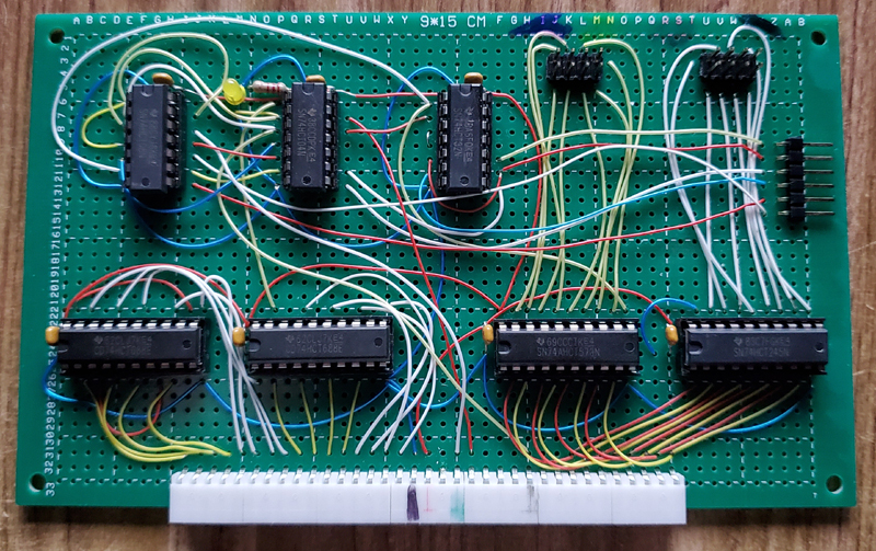
I've recently completed the new software front panel I/O card to replace some of the functionality provided by the 6522 parallel I/O card. The goal was to eliminate the need for an expensive chip to read the 8 data switches and drive 8 additional LEDs. The complex functions that the 6522 was capable of were being underutilized in that task, and I realized I could achieve the same goal in 7400 series logic. The result is a card which adds in 3 new features, recreates a previously dismissed feature, and frees up the parallel I/O card for more powerful tasks.
|
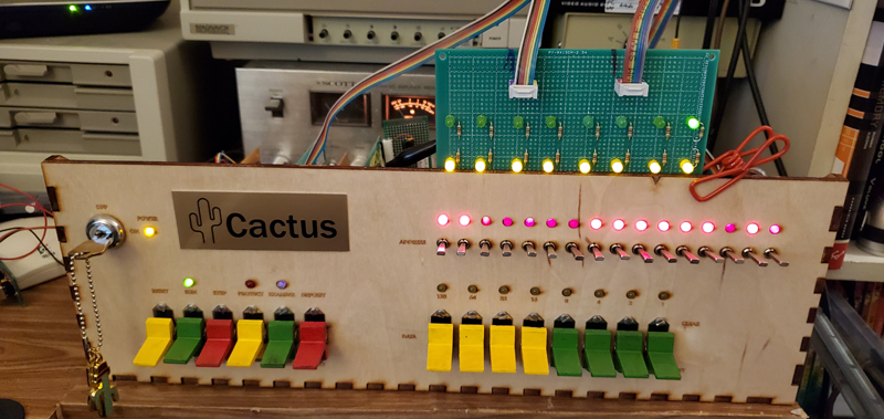
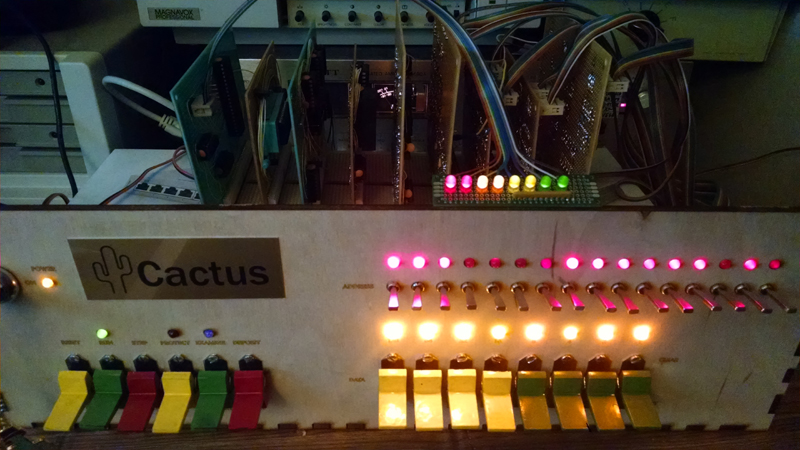
First, there is a buffer to directly link the data bus to a bank of LEDs so that the user can watch the data bus at all times. However, I didn't have any remaining room on the original front panel, so I created an addendum board to tack onto the front panel for the time being. The row of yellow LEDs is the data bus indicator bank. Above that is a row of green LEDs, which is the software controlled LED bank. An 8-bit latch stores the value to be displayed here, and is a write-only location.
|
The software front panel I/O card includes control logic to replace the logic present on the Data Control card in order to allow the new complex functionality. Since the Data Control card already includes 8 flip flops to keep track of the momentary switches, I decided to reuse this logic, or rather, supplement it. Normally, all of the front panel DMA control logic is locked out when the CPU is running as both a safety measure and to prevent bus contention. Using a complex lockout chain to maintain existing DMA functionality, I've created a way for the CPU to access that same data while it's running.
However, one thing that concerned me was the inability to discern between two distinct switch presses on a system that latches switch presses and provides no facility for interupt requests. My solution was to allow the CPU the ability to clear all 8 flip flops whenever that memory location is written to instead of read from. In fact, three distinct functions all exist on a single address. When you write to 0xA900, you clear the flip flops, but also write a value to the software controlled LED bank. When you read from 0xA900, you check the state of the 8 flip flops. Admittedly it's a bit of an irregular control method, so if it proves to be troublesome, I will end up separating these functions between two addresses.
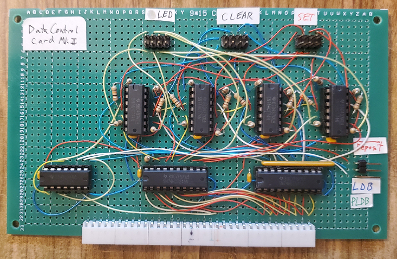
I've also recently revised the Data Control and Status Control cards. The new Data Control card eliminates a 2 buffers and a significant number of wires. On the Status Control card, I've improved the reliability of the sequence chains for Examine/Examine Next/Deposit Next. This was done using some one-shot 7474s to ensure only a single clock pulse enters what is effectively a modified ring counter. The changes come in the form of a riser board attachment.
The Data Control card no longer indicates what was happening directly on the data bus, which is fine since the software front panel I/O card now exists to serve that purpose.
|
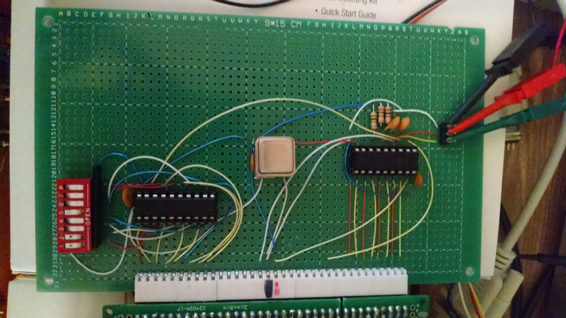
I've improved the single step clock circuitry. I have implemented a pair of monostable multivibrators to send a complete clock pulse down the bus. Tests indicated that the VIA and ACIA were ignoring instructions from the CPU I discovered that the clock pulses never went LOW, and clocked I/O devices need a complete LOW/HIGH cycle. RAM and ROM aren't clocked devices, and the CPU is the feeding the clock, so operations that ignored I/O worked fine in the previous implementation of single step mode. However, since installng a 74HCT123, these I/O devices respond to single stepping. It's amazing how many cycles it takes for BASIC to send text over serial.
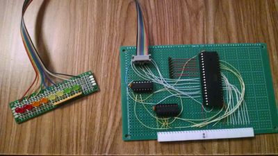
I've built a simple 6522 board, and it's been tested with a modern CMOS 65C22. While it is no longer used in this capacity, I've added a bank of 8 software-controlled LED, and another bank of headers. I had integrated the 8 data switches on the front panel into the 6522 for use with software input, however, this only worked with the previous generation of data control card which has now been retired.
|
|
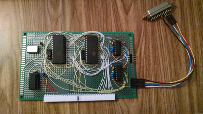
I'm also testing a new serial board that uses two 6551 ACIA's with MAX232 level shifters all on a single card. Due to the significantly reduced part count for baud rate selection, I was able to fit the second serial port I've desired for some time. At present, I've got one of the ACIA's functional, and have modified the serial routines for BASIC to utilize the new chip. The user can now change the baud rate in software, rather than physically moving a jumper. I was having decent luck with it for awhile, then it stopped cooperating. The second ACIA has yet to be seriously tested.
|
I was curious about running the Cactus with an authentic NMOS 6502 manufactured by Commodore. This meant adding buffers for the address and data buses to silence the CPU during front panel interaction. However, the nature of the internal registers will limit the functionality with this microprocessor variant. Ultra-slow clock modes, single stepping, and stopping the CPU expecting to resume on a human timescale will be out of the question on the NMOS board. Testing has proven that the R/W line also requires a buffer to prevent data from being clobbered during front panel DMA, and modifications to account for this have been implemented. The NMOS board runs at either 1MHz or 50KHz.
Meanwhile, the CMOS board was tested with a 2MHz clock and a 2.457MHz clock. The speed of the machine is ultimately limited by the 6551's rather than the 65C02, the latter of which can operate at up to 14MHz. The current fastest the Cactus has operated at is 2.457MHz, but the design was never intended to operate above 1MHz.
|
Experiments are also taking place involving 8-bit latches, DACs, and other electronic components that I'm less familiar with. A recent revelation about the SAA-1099 sound chip in particular has resulted in a bit of fresh look at interfacing with it. I've built a crude sound card around one of them, and have begun basic testing. It could probably use an amplifier, but for the moment it will have to use the amplification of an external device. Test routines of random instructions have produced promising results.
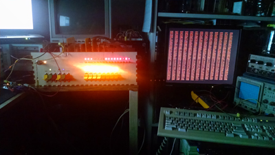
The Cactus in action, running BASIC, with its older case badge.
|
|
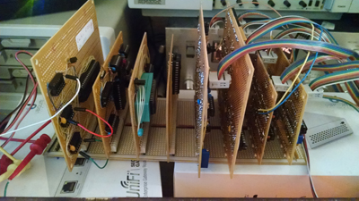
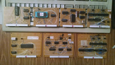
The heart and soul of the Cactus: the 35 pin backplane, and the 7 primary cards.
Top row: RAM card, EPROM card, serial card, address control card (rev 1)
Bottom row: CPU card, status control card, data control card
|
|
Front Panel Logic Cards
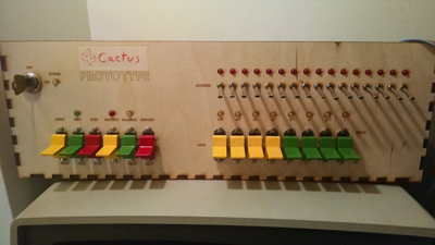
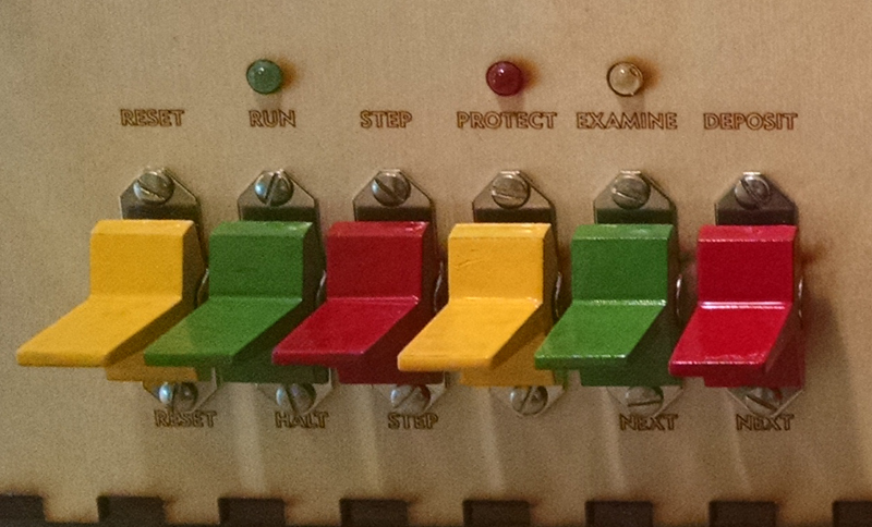
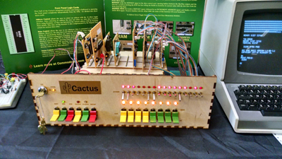
Over half of the Cactus's integrated circuitry is dedicated to operating the front panel independently from the 6502. It's divided into three main cards:Address Control allows the user to select an address to visit using the 16 silver toggle switches. After selecting an address, the user can either see what data is located there using Examine, or they can increment the current address just by using the Examine Next switch. This time saving measure is complemented by the Deposit Next switch for serious data entry.
Data Control allows the user to see whatever data is contained at the selected address. However, the data bus is not directly wired to the status lights. Instead, a series of interlocking buffers are used to load that value into a series of flip-flops, used as a temporary workspace. From there, the user can modify a byte, one bit at a time using SET & CLEAR momentary switches. When the user has finished entering a new byte or modifying an existing byte, pressing Deposit will allow that byte to pass back to the data bus and overwrite the previous value in RAM. This allows the user to fix off-by-one errors with greater ease. While the microprocessor is in control, the data bus is directly visible on the data indicators.
Status Control allows the user to control complex operations of the machine. All of the status control switches are momantaries, with accompanying flip-flops or debounce circuitry. The Address & Data control card functions are both orchestrated by the Status Control card, to ensure that each operation happens in the correct order. Sequencing is governed by a logic chain of cascading D-latches clocked from a 555 timer. Many of the direct memory access safety interlocks are controlled from here.
Front Panel Switches
|
|
Watch the Cactus during an earlier stage of development:
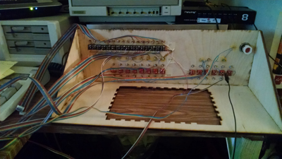
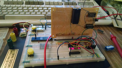
So many wires, so many tests...
|
|
Vintage Computer Festival East XIII
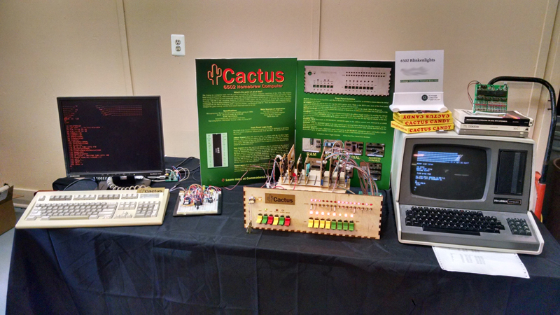
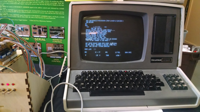
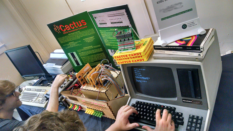
The Cactus was on display at Vintage Computer Festival East XIII in Wall, NJ on May 19 & 20, 2018. I explained why I built it, what motivations lead it its design choices, and where the project was headed. Visitors were welcome to try using the front panel, program in BASIC, and listen to me ramble. I used a Heathkit H89 as a serial terminal to program using BASIC. A friend connected up a dot matrix printer in parallel with the terminal, and also managed to copy over Lunar Lander one line at a time from my Toshiba Libretto 70CT. Playing games on the Cactus!I also briefly replaced the 1MHz clock crystal with an external pulse generator. The system clock was brought down into the sub-100KHz range, going as low as a few dozen Hz at times just for fun. I garuntee you've never seen a 6502 move that slowly. BASIC runs really slowly at that speed, and it gives you some perspective on how much work is happening in such a brief moment in time within the 6502.
A friend filmed the Cactus while I had external pulse generator connected. You can see individual instructions go by on the indicators as it struggles to begin rendering text on my H89:
|
|
|
|
Despite not actually being a vintage computer, it was a major hit with visitors and fellow exhibitors. Quite frankly, I wasn't expecting such an overwhelmingly positive response.
Click here to view my photos from VCF East XIII
Vintage Computer Festival West 13
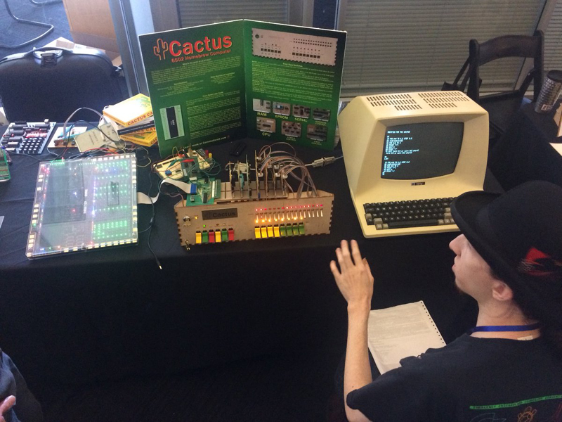
I exhibited the Cactus at VCF West on August 4th & 5th in Mountain View California, at the Computer History Museum. This was my first time at VCF West, and the atmosphere made for a different experience compared to VCF East. Erik Klein was kind enough to lend me the use of a Televideo 910 due to my considerable distance from home. The Cactus was transported in a customized flight case to ensure it arrived intact. However, due to poor packing on my part, the contents shifted on its 3000 mile journey. The Deposit switch and a pair of header pins on the Status Control card were damaged in transport, and required on-site repairs before the show began. Fortunately, I was able to effect repairs, and the rest of the weekend's demonstrations went smoothly.A few weeks prior to the show, I discovered that the MOnSter 6502 would be in attendance, along with the good folks at Evil Mad Scientist Laboratories. I reached out to its creator, Eric Schlaepfer, and asked if he would be willing to combine our two machines in an experiment. He was interested, letting me know that as long as I adhered to the NMOS specification and clocked down to 50KHz, the two should be able to work together. Normally, the Cactus relies on the 65C02's Bus Enable pin to halt the CPU and allow the front panel logic to take over to provide the user with direct memory access. I built a new processor card with additional buffers to account for the lack of such a pin on the NMOS variant, and tested it with an original Commodore 6502 from 1983.
Once at VCF West, our first attempt on Saturday pointed out that I had neglected to buffer the Read/Write line, resulting in bus contention. On Sunday, Eric brought me a breadboard, some additional jumper wires, and a few tristate buffers from his stockpile. After splicing an additional 74LS245 into the NMOS card, and testing with an NMOS 6502, we decided to try again. Lo and behold, the Cactus and the MOnSter 6502 successfully booted into BASIC, and ran at 50KHz for about half an hour, creating a spectacular fusion of blinkenlights. That makes the Cactus the third machine to use the MOnSter 6502, and the first one that wasn't made by Eric. Needless to say, this was the highlight of my weekend.
|
Click here to view my photos from VCF West XIII
DEFCON 26 Hardware Hacking Village
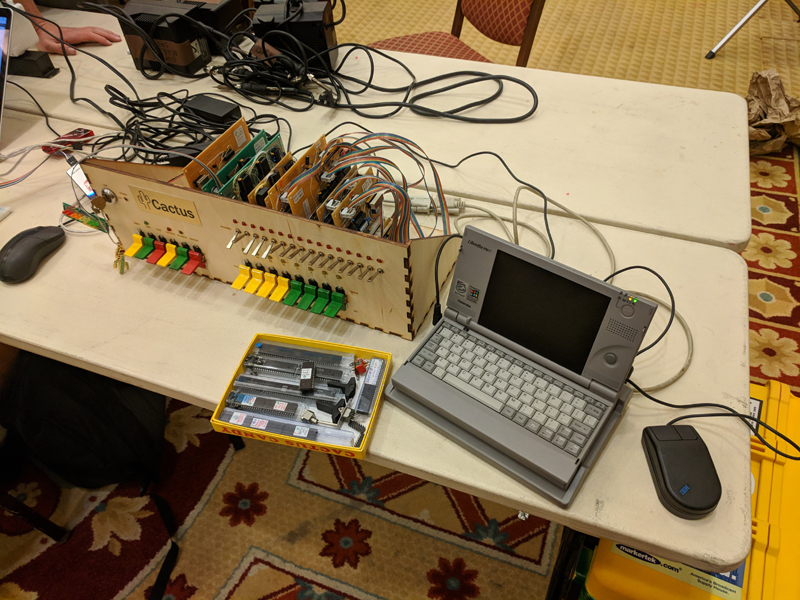
I gave a talk & demonstration at the DEFCON 26 HHV at 4PM on August 11th. I discussed the history of the front panel and 6502 machines, my design influences and inspirations, and demonstrated the machine in action. I was really happy with the level of interest on display by attendees. This time, the Cactus made it to the show in one piece and performed admirably. Out of respect for the DEFCON photo policy, I ended up with a very small amount of photos overall.
|
Click here to download the video!
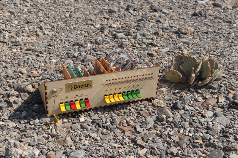
Here's a photo from the desert photoshoot I did before DEFCON got into full swing. Special thanks to 3Chip for taking these desert photos, and assisting me at DEFCON as the official Cactus Goon.

|
Vintage Computer Festival Midwest 13
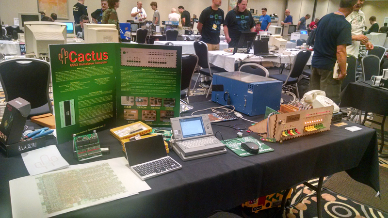
I exhibited the Cactus at VCF Midwest , September 15th & 16th in Elk Grove Village, Illinois. I also gave a talk on the subject, along with a history of various front panels to add some context to my project. If you're interested in watching me speak on the subject, the entirety of my talk is available courtesy of the VCFMW folks.
|
Click here to view my photos from VCF Midwest 13
Vintage Computer Festival East XIV
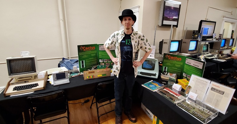
I exhibited the Cactus a second time at VCF East XIV in Wall, NJ on May 4 & 5, 2019. I focused on displaying the improvements from last year, as well as providing historical context for the Cactus compared to other 1970s front panels with 6502's. Bill Sudbrink lent me an authentic OSI-300, Bill Degnan lent me a CGRS Microtech 6502 front panel (which may end up being for the matching S-100 card rather than the SYM-1), and TangentDelta lent me his ADM-3A (as a last minute replacement for my upset H89). Singularity assisted me in setting up and running my exhibit table for the duration of the weekend. Many thanks to all of them for thier help!The Cactus's more robust front panel logic performed admirably, and the Cactus Seed (the minimal, test board) made its functional debut running the terminal for a significant chunk of time. Software controlled I/O and even the sound card were demonstrated at various points. I brought along an OSI Challenger 4P as a point of reference on the same BASIC used by the Cactus, to show the direction that 6502 kit machines went following the advent of the appliance home computer in 1977.
I was part of a panel discussion on Friday with Glitch & Bill Dudley on the subject of homebrew computing. We gave our perspectives on our projects, and answered questions from the audience.
|
Click here to view my photos from VCF East XIV
Vintage Computer Festival West XIV
I exhibited the Cactus at VCF West XIV in Mountain View, CA on August 3rd and 4th. Due to the limitations of checked airline bags, I had to reduce the exhibit's contents compared to VCF East. However, I still wanted to capture the forgotten history of 6502 front panels. For the second year in a row, Erik Klein lent me a Televideo 910 terminal to use which was much appreciated.
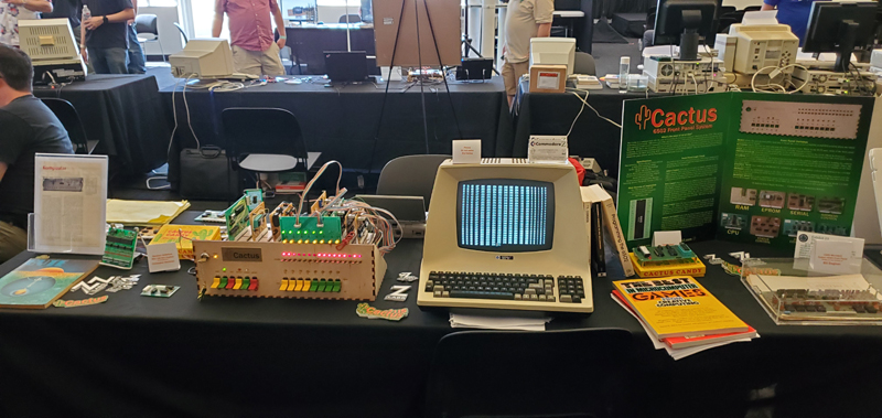
|
Once again, Eric Schlaepfer's exhibit booth was directly next to mine, so we bolted the MOnSter 6502 into the Cactus to demonstrate the interoperability of the two machines. Fortunately this time it was a simple plug & play approach, and everything worked great.
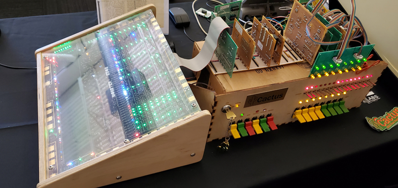
|
For the duration of the weekend, the Cactus performed reliably for visitor demos. I was asked some interesting questions by visitors, including a reporter from KQED. Most notably, I was interviwed by a popular vintage technology personality on youtube, AkBKuKU. He does a great job covering the feel of the event, and even recorded the MOnSter Cactus experiment. It was a blast!
Click here to view my photos from VCF West XIV
Vintage Computer Festival Midwest 14
I attended VCF Midwest 14 in Elmhurst, IL on September 14th and 15th, in its new, larger venue. Once again, I exhibited the Cactus, providing demonstrations, and giving others an opportunity to experience the front panel. The game 'ZNEK" by ZephyrZ80 was on display, and proved to be a hit! The high score is currently held by TX_Dj with 23 points. Thank you again to TangentDelta for lending me his blue ADM-3A to use as my terminal for the weekend. Thank you to all who attended and took the time to see the Cactus, and speak with me about the project.
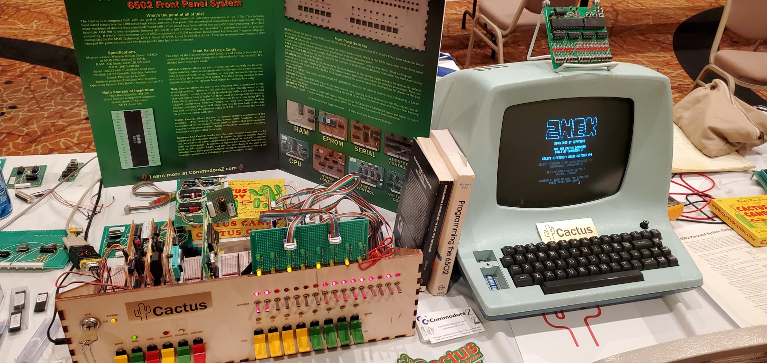
|
Click here to view my photos from VCF Midwest 14
I've been asked at multiple events if I'm planning to make a kit version of the Cactus. Right now the answer is "Probably." I would love to be able to make a kit version of the Cactus for those interested. Please be patient, I've got a lot of work to do before we're at that stage of development. I have no intention of selling anything until I have a design I'm confident in. I'm talking with friends who have produced and sold kits about what's involved. How many people want a Cactus? How many kits would that be? How much would they cost? These are questions I'm working towards answering. As of right now, I've got atleast a dozen interested parties. If you are interested in a kit when they're ready, send me an email to let me know. |
Have a question? Want to know more about the Cactus? Know of another 6502 machine with a front panel? Email me:

Home
This page was last updated on 8-26-2023